| Research
and Interests |
|
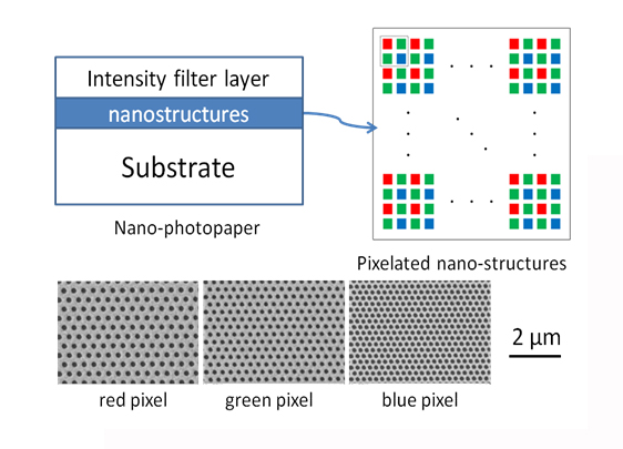
Nanostructure Color PrintingWith the advancement of nanotechnology in recent years, efforts and activities have started to be geared toward the implementation of nanostructures in generating vibrant, vivid colors with super high resolution. Traditionally, colors are generated mainly based on absorption of light at a certain band from pigments and dyes. They are usually chemically instable (color fading) and pose environmental concerns. Nanostructure colors, on the other hand, which generate colors based on interaction of light with optical nanostructures, have started to facilitate to replace traditional colors. From specially engineered nanostructures, distinctive bright iridescent colors can be displayed from pixels in the size as small as 250 nm!!! Nanostructure color printing allows color images to be printed at unprecedented resolution and information to be optically stored at incredibly high density. At CiBERLAB, we design and fabricate nanostructure color pixels with unique optical properties and apply these nano-pixels in printing color images. Through our revolutionary top-down approaches, color images can be printed with super-high throughput which allows them to be used in increasingly wide variety of real-world applications: customizable security and authentication features; print-and-paste transparent full-color panel; eye-readable optical archival storage; specialty color-decorative films for power-generation panels; high-resolution multi-direction optical displays. It is a perfect combination of nanoscale coloration with high-speed micropatterning technique and paves the way for realizing next-generation main-stream color printing technology. Four technologies in nanostructure color printing that were developed in CiBERLAB will be introduced in the following: MIONS printing; eye-readable full-color permanent optical archival storage; NANO-ART; multi-directional full-color optical display enabled by plasmonic printing.MIONS printingCiBERLAB has invented the Molded-Ink-on-Nanostructured-Surfaces (MIONS) printing, which is a scalable, high-throughput nano-manufacturing technique based on inkjet printing of nanoparticles on pre-fabricated nanostructured surfaces. Our developments have been published in two papers in prestigious high-impact journal ACS Nano (Hao Jiang et al., "Molding inkjetted silver on nanostructured surfaces for high-throughput structural color printing", ACS Nano 10 (11), pp. 10544-10554, 2016; Hao Jiang et al., "Scalable inkjet-based structural color printing by molding transparent gratings on multilayer nanostructured surfaces", ACS Nano 12 (4), pp. 3112-3125, 2018). One patent has already been allowed in Canada (Hao Jiang, and Bozena Kaminska, Canada Patent Application CA2949589). In MIONS printing, a transparent polymer metasurface comprised of nanostructures is first replicated from a stamp using low-cost nanoimprint process. On the polymer metasurface, metallic or dielectric nanoparticles are then inkjet-printed and "molded" into nanostructures that give special nano-optical properties controllable through the nanostructure geometries. These "molded" nanostructures comprise a customizable metasurface to store optical information. Based on MIONS printing, various types of specially engineered optical metasurfaces can be realized and manufactured in large volume with low cost. Our invention has received considerable interests from academic society and industrial collaborators. It has been highlighted in Chemistry & Engineering News (https://goo.gl/tMmxhh) and Advances in Engineering website (https://goo.gl/QcMVLW). Currently, we focus on applications in customizable security features, transparent displays and specialty decoration color films. The actual applications using MIONS printing are boundless and could potentially be applied in the color printing for office use in the near future.Eye-Readable full-color permanent optical archival storageExisting main-stream optical storage devices can store high-density information (e.g., Blu-Ray DVDs), however, as the technology advances, many stored data cannot be read out, simply because the reader devices will become obsolete. At a global scale, huge cost is spent yearly to migrate data into a new generation of storage device. For storing key information that has historical, scientific, legal and cultural value, optical storage that can always be accessed is in demand. To provide a viable solution, CiBERLAB invented a solvent-free technique using low-power diode laser to directly write and record structural colors onto pixelated metasurfaces. Owing to the excellent chemical stability of the structures, the colors are projected to last very long and there is no need for data migration. This work has been published in a newly-launched high-impact journal Nano Futures (Hao Jiang et al., "Solvent-free optical recording of structural colours on pre-imprinted photocrosslinkable nanostructures", Nano Futures 1, p. 025001, 2017). This technology has also been highlighted in a news story in NanoTechWeb (https://goo.gl/YvRWQr). In the next stage, we are collaborating with industrial partners in scaling up the production using industrial-grade lasers to store security archival images and personalized information on personal ID cards.NANO-ARTIn most forms, artworks utilize colors to present an artist's view of world. With nanostructures, unique colors and viewing effects can be achieved, and therefore unique arts can be produced based on nanostructures. At CiBERLAB, we initiated the exploration of using nanostructure colors in artworks, in collaboration with professional artists. In 2014, our group demonstrated, for the first time, printing journal covers for an academic journal PUBLIC for celebrating the 50th anniversary using nanostructures. In the following, we have introduced a new form of art, named "NANO-ART" based on colorful nanostructures. In 2015, we demonstrated (in collaboration with Scott Lyall) world's first photo-size NANO-ART color image, exhibited in prestigious art gallery Miguel Abreu in New York City, U.S.. In 2017, we have produced numerous NANO-ART images for Scott Lyall's a full-scale art show "DRAGONS" at Campoli Presti gallery in London, UK. In producing these artworks, the throughput and cost is the key. Through the research at CiBERLAB, we have made breakthrough in the patterning technique to enable producing artworks cost-effectively. Our developed technologies used in producing NANO-ART have been published in patents and journals (Hao Jiang et al., U.S. Patent US9460665B2; Hao Jiang et al., U.S. Patent US9696468B2; Mohamad Rezaei, Hao Jiang, and Bozena Kaminska, "Structural colour printing from a reusable generic nanosubstrate masked for the target image", Nanotechnology 27 (8), p. 085301, 2016.)Multi-directional full-color optical display enabled by plasmonic printingFull 3-D glassless full-color displays have been demanded for long time. However, the challenge in devising them for real-world applications are daunting, considering the complexity in the design and engineering of such displays. One approach that seems to be within rich is the multi-directional optical display that allows viewers to see different frames in different directions to render into a full 3-D view. Microlens, is among the most promising candidates for multi-directional displays. It has been already widely applied in security and authentication applications, for example, the black/white security thread showing movement effects on the 100-US-dollar banknotes. To embed multiple frames, patterns must be printed into a resolution higher than 5,080 dots per inch (DPI). However, such a resolution is not yet attainable through conventional color printing techniques and therefore the displayed patterns on banknotes were so far restricted to black/white images. CiBERLAB developed a plasmonic color printing technique based on electron beam lithography and nanoimprint lithography, and the achieved resolution is higher than 12,700 DPI. The attained full color patterns can be rapidly replicated at industrial scale using roll-to-roll UV embossing. Currently, this technique is being scaled up to enable over 100 full-color frames through microlens arrays. |